


By: Evan R. (evan.delete@this.no-email.com),
Room: Moderated Discussions
Nick M (nick.delete@this.anon.com) on February 2, 2026 7:17 pm wrote:
> How does this proposal reduce load latency compared to Granite Rapids?
On Granite Rapids, handling an L2 miss for a cache line held in a private cache of a different CPU core consists of the following steps:
1. CPU core sends read request over Network-on-Chip (NoC) to Caching Home Agent (CHA) responsible for cache line
2. CHA uses snoop filter to determine that cache line is in private cache of a different CPU core
3. CHA sends read request over NoC to CPU core that holds cache line
4. CPU core that holds cache line sends it over NoC to requesting core
With my proposal for Coral Rapids, the steps would be:
1. CPU core sends read request to CPU hub over a direct link
2. CPU hub uses snoop filter to determine which CPU core holds cache line
3. CPU hub sends read request to CPU core that holds cache line over a direct link
4. CPU core that holds cache line sends it over NoC to requesting core
On microarchitectures like Granite Rapids, there are 3 transfers over the NoC to load from a private cache of a different CPU core. With my proposal, there is only one transfer over the NoC for that operation. My proposal uses direct links between a CPU hub and the 16 CPU cores on a CPU chiplet to eliminate 2 transfers over the NoC. If the cache line is held in an L3 slice, only one transfer over the NoC would be eliminated with my proposal.
Correction to my original proposal: The links between the CPU hub and the 16 CPU cores on a CPU chiplet would consist of one physical address tag (currently 46 bits) in each direction, one 8-bit CPU core identifier plus a few control signals. This would allow a CPU core to sustain one load per clock from L3 cache or DRAM. When going from the CPU hub to a CPU core (step 3 above), the 8-bit CPU core identifier tells where to send the cache line.
On Granite Rapids, a DRAM read consists of the following steps:
1. CPU core sends read request over NoC to CHA responsible for cache line
2. CHA uses snoop filter to determine that cache line is not in on-chip caches
3. CHA sends read request over NoC to DRAM controller
4. DRAM controller reads cache line and sends it over NoC to requesting core
With my proposal for Coral Rapids, the steps would be:
1. CPU core sends read request to CPU hub over a direct link
2. CPU hub uses snoop filter to determine that cache line is not in on-chip caches
3. CPU hub sends read request to base hub over a direct link
4. DRAM controller attached to base hub reads cache line and sends it over NoC to requesting core
On microarchitectures like Granite Rapids, there are 3 transfers over the NoC to load from DRAM. With my proposal for Coral Rapids, there is only one transfer over the NoC to load from DRAM. My proposal uses direct links from each of the 16 CPU cores on a CPU chiplet to a CPU hub and a direct connection from a CPU hub to a base hub attached to a DRAM controller to eliminate 2 transfers over the NoC.
Each CPU hub would only be used for loads and instruction fetches that miss in the L2 cache. Stores would transfer both the address tag and the cache line data over the NoC.
> How would the 4 HBF stacks and 2 HBM stacks be connected to the 4 base chiplets given that 6 is not a multiple of 4?
Each of the 2 PCIe/accelerator chiplets would be attached to 2 HBF stacks and one HBM stack. The PCIe/accelerator chiplets would contain memory controllers for HBF and HBM. Each PCIe/accelerator chiplet would connect data from one HBM stack to two base chiplets (a Y shape connection). Each base chiplet would also have a high-speed connection to data from one HBF stack. Once data from HBF and HBM is on a base chiplet, it would be wired to the crossbar that connects the 4 CPU chiplets on a base chiplet.
A bi-directional ring connecting 4 nodes has 4 links while an all-to-all mesh connecting 4 nodes has 6 links. The all-to-all mesh has fewer network stops than a bi-directional ring (1 hop vs 1 or 2 hops). For a fixed number of EMIB connections between base chiplets, the links for a bi-directional ring would be wider than the links for an all-to-all mesh. However, in the same way that airlines use connecting flights when a direct flight is full, if a link in an all-to-all mesh is full, a 2 hop connection could be used instead. It therefore seems to me that an all-to-all mesh might be a better way to connect the 4 base chiplets than a bi-directional ring. I don't know enough about the relative size of the wire delay, EMIB delay and network stop delay to have an opinion about the best approach. If the network stops are a small fraction of the total delay, that would favor a bi-directional ring. If network stops are a significant fraction of the total delay, that would favor an all-to-all mesh.
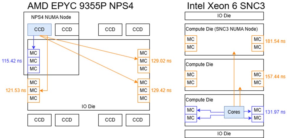
A clue about whether network stops add significant delay is in the diagram shown above. Turin has a 14ns difference in DRAM latency between DRAM controllers close vs far from a Global Memory Interconnect port. That suggests the wire delay across AMD's IO die is 14ns. Granite Rapids has a 24 to 25ns increase in DRAM latency from each chiplet that is crossed to reach a DRAM controller. That indicates that the wire delay + EMIB delay + mesh stop delays across one Granite Rapids chiplet is 24 to 25ns. Granite Rapids has a total of 128 cores on 3 chiplets, so 43 cores per chiplet. If the mesh on a chiplet is organized as 9 x 5, there would be 5 mesh stops to cross a chiplet. If the wire delay + EMIB delay is zero, Granite Rapids would have 5ns per mesh stop. Since the wire delay + EMIB delay is not zero, one mesh stop might be adding about 2 to 3ns. For the case of comparing an all-to-all mesh vs a bi-directional ring to connect the 4 base chiplets in my proposal for Coral Rapids, a bi-directional ring is only adding at most one network stop so I'd guess a bi-directional ring is better but I'm still not 100% sure. A bi-directional ring maximizes the bandwidth between base chiplets provided by a fixed number of EMIB connections since diagonal connections to connect a square of 2x2 base chiplets use 2 EMIB connections each.
Each of the base chiplets in my Coral Rapids proposal holds 64 CPU cores. To handle a burst of loads from one base chiplet to another base chiplet, instead of the dedicated connections between base hubs mentioned in my original proposal, the connections used to transfer cache lines between base chiplets could be used to transfer 10 load requests (address tag + CPU core identifier) instead of one cache line + address tag + CPU core identifier.
Sub-NUMA clustering will be essential to get good performance on a processor with 256 CPU cores. AMD's 3D V-Cache has proven to be a very effective way of increasing the L3 cache capacity. I think sub-NUMA clustering and optional 3D V-Cache would be a strong combination for Coral Rapids assuming Intel improves Xeon's L3 latency and DRAM latency. There are 12-high stacks of DRAM die for HBM in mass production today so Intel should be able to stack (one or two 3D V-Cache die) + base die + CPU die.
AMD's MI300 and MI350 series accelerators have 256 MB of memory-side cache built on 6nm base die. At CES 2026, AMD said their upcoming MI400 series has 3nm base die and 1.5x more HBM stacks than the MI300 and MI350 series. It therefore seems reasonable to guess the memory-side cache of the MI400 series will be 384 MB. For Zen 6 Venice or Zen 7 Verano, AMD could provide the option of a 384 MB L4 memory-side cache and 12 stacks of HBM/HBF. The 8 compute die would be some combination of CPU and GPU compute die to make the MI400A or MI500A. AMD could also make a half-size version with 4 CPU die and 6 stacks of HBM/HBF for applications such as in-memory databases (e.g. SAP HANA). A half-size version with 2 CPU die and 2 GPU die could be used for a mini-DGX Station or a robot brain.
> How does this proposal reduce load latency compared to Granite Rapids?
On Granite Rapids, handling an L2 miss for a cache line held in a private cache of a different CPU core consists of the following steps:
1. CPU core sends read request over Network-on-Chip (NoC) to Caching Home Agent (CHA) responsible for cache line
2. CHA uses snoop filter to determine that cache line is in private cache of a different CPU core
3. CHA sends read request over NoC to CPU core that holds cache line
4. CPU core that holds cache line sends it over NoC to requesting core
With my proposal for Coral Rapids, the steps would be:
1. CPU core sends read request to CPU hub over a direct link
2. CPU hub uses snoop filter to determine which CPU core holds cache line
3. CPU hub sends read request to CPU core that holds cache line over a direct link
4. CPU core that holds cache line sends it over NoC to requesting core
On microarchitectures like Granite Rapids, there are 3 transfers over the NoC to load from a private cache of a different CPU core. With my proposal, there is only one transfer over the NoC for that operation. My proposal uses direct links between a CPU hub and the 16 CPU cores on a CPU chiplet to eliminate 2 transfers over the NoC. If the cache line is held in an L3 slice, only one transfer over the NoC would be eliminated with my proposal.
Correction to my original proposal: The links between the CPU hub and the 16 CPU cores on a CPU chiplet would consist of one physical address tag (currently 46 bits) in each direction, one 8-bit CPU core identifier plus a few control signals. This would allow a CPU core to sustain one load per clock from L3 cache or DRAM. When going from the CPU hub to a CPU core (step 3 above), the 8-bit CPU core identifier tells where to send the cache line.
On Granite Rapids, a DRAM read consists of the following steps:
1. CPU core sends read request over NoC to CHA responsible for cache line
2. CHA uses snoop filter to determine that cache line is not in on-chip caches
3. CHA sends read request over NoC to DRAM controller
4. DRAM controller reads cache line and sends it over NoC to requesting core
With my proposal for Coral Rapids, the steps would be:
1. CPU core sends read request to CPU hub over a direct link
2. CPU hub uses snoop filter to determine that cache line is not in on-chip caches
3. CPU hub sends read request to base hub over a direct link
4. DRAM controller attached to base hub reads cache line and sends it over NoC to requesting core
On microarchitectures like Granite Rapids, there are 3 transfers over the NoC to load from DRAM. With my proposal for Coral Rapids, there is only one transfer over the NoC to load from DRAM. My proposal uses direct links from each of the 16 CPU cores on a CPU chiplet to a CPU hub and a direct connection from a CPU hub to a base hub attached to a DRAM controller to eliminate 2 transfers over the NoC.
Each CPU hub would only be used for loads and instruction fetches that miss in the L2 cache. Stores would transfer both the address tag and the cache line data over the NoC.
> How would the 4 HBF stacks and 2 HBM stacks be connected to the 4 base chiplets given that 6 is not a multiple of 4?
Each of the 2 PCIe/accelerator chiplets would be attached to 2 HBF stacks and one HBM stack. The PCIe/accelerator chiplets would contain memory controllers for HBF and HBM. Each PCIe/accelerator chiplet would connect data from one HBM stack to two base chiplets (a Y shape connection). Each base chiplet would also have a high-speed connection to data from one HBF stack. Once data from HBF and HBM is on a base chiplet, it would be wired to the crossbar that connects the 4 CPU chiplets on a base chiplet.
A bi-directional ring connecting 4 nodes has 4 links while an all-to-all mesh connecting 4 nodes has 6 links. The all-to-all mesh has fewer network stops than a bi-directional ring (1 hop vs 1 or 2 hops). For a fixed number of EMIB connections between base chiplets, the links for a bi-directional ring would be wider than the links for an all-to-all mesh. However, in the same way that airlines use connecting flights when a direct flight is full, if a link in an all-to-all mesh is full, a 2 hop connection could be used instead. It therefore seems to me that an all-to-all mesh might be a better way to connect the 4 base chiplets than a bi-directional ring. I don't know enough about the relative size of the wire delay, EMIB delay and network stop delay to have an opinion about the best approach. If the network stops are a small fraction of the total delay, that would favor a bi-directional ring. If network stops are a significant fraction of the total delay, that would favor an all-to-all mesh.
A clue about whether network stops add significant delay is in the diagram shown above. Turin has a 14ns difference in DRAM latency between DRAM controllers close vs far from a Global Memory Interconnect port. That suggests the wire delay across AMD's IO die is 14ns. Granite Rapids has a 24 to 25ns increase in DRAM latency from each chiplet that is crossed to reach a DRAM controller. That indicates that the wire delay + EMIB delay + mesh stop delays across one Granite Rapids chiplet is 24 to 25ns. Granite Rapids has a total of 128 cores on 3 chiplets, so 43 cores per chiplet. If the mesh on a chiplet is organized as 9 x 5, there would be 5 mesh stops to cross a chiplet. If the wire delay + EMIB delay is zero, Granite Rapids would have 5ns per mesh stop. Since the wire delay + EMIB delay is not zero, one mesh stop might be adding about 2 to 3ns. For the case of comparing an all-to-all mesh vs a bi-directional ring to connect the 4 base chiplets in my proposal for Coral Rapids, a bi-directional ring is only adding at most one network stop so I'd guess a bi-directional ring is better but I'm still not 100% sure. A bi-directional ring maximizes the bandwidth between base chiplets provided by a fixed number of EMIB connections since diagonal connections to connect a square of 2x2 base chiplets use 2 EMIB connections each.
Each of the base chiplets in my Coral Rapids proposal holds 64 CPU cores. To handle a burst of loads from one base chiplet to another base chiplet, instead of the dedicated connections between base hubs mentioned in my original proposal, the connections used to transfer cache lines between base chiplets could be used to transfer 10 load requests (address tag + CPU core identifier) instead of one cache line + address tag + CPU core identifier.
Sub-NUMA clustering will be essential to get good performance on a processor with 256 CPU cores. AMD's 3D V-Cache has proven to be a very effective way of increasing the L3 cache capacity. I think sub-NUMA clustering and optional 3D V-Cache would be a strong combination for Coral Rapids assuming Intel improves Xeon's L3 latency and DRAM latency. There are 12-high stacks of DRAM die for HBM in mass production today so Intel should be able to stack (one or two 3D V-Cache die) + base die + CPU die.
AMD's MI300 and MI350 series accelerators have 256 MB of memory-side cache built on 6nm base die. At CES 2026, AMD said their upcoming MI400 series has 3nm base die and 1.5x more HBM stacks than the MI300 and MI350 series. It therefore seems reasonable to guess the memory-side cache of the MI400 series will be 384 MB. For Zen 6 Venice or Zen 7 Verano, AMD could provide the option of a 384 MB L4 memory-side cache and 12 stacks of HBM/HBF. The 8 compute die would be some combination of CPU and GPU compute die to make the MI400A or MI500A. AMD could also make a half-size version with 4 CPU die and 6 stacks of HBM/HBF for applications such as in-memory databases (e.g. SAP HANA). A half-size version with 2 CPU die and 2 GPU die could be used for a mini-DGX Station or a robot brain.
Thread (12 posts)
| Topic | Posted By | Posted |
|---|---|---|
| Proposal for Xeon Coral Rapids | Evan R. | |
| Proposal for Xeon Coral Rapids | Nick M | |
| Proposal for Xeon Coral Rapids | anonymou5 | |
| Proposal for Xeon Coral Rapids | tidtx | |
| Proposal for Xeon Coral Rapids | Evan R. | |
| Proposal for Xeon Coral Rapids | anon2 | |
| Proposal for Xeon Coral Rapids | Evan R. | |
| Proposal for Xeon Coral Rapids | anon2 | |
| Proposal for Xeon Coral Rapids | Heikki Kultala | |
| Proposal for Xeon Coral Rapids | Anon4 | |
| Proposal for Xeon Coral Rapids | Evan R. |