


By: Heikki Kultala (heikki.kulta.la.delete@this.gmail.com),
Room: Moderated Discussions
Evan R. (evan.delete@this.no-email.com) on January 28, 2026 4:01 am wrote:
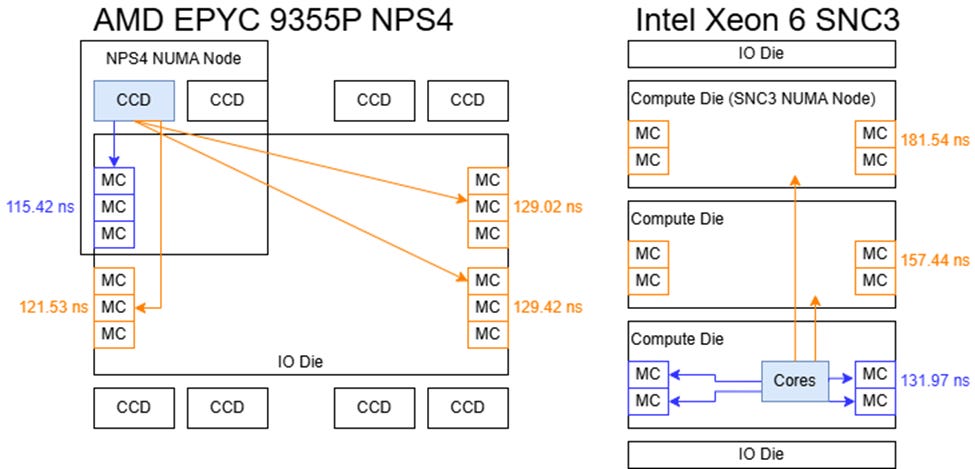
> According to the Chips and Cheese measurements shown below, EPYC Zen 5 Turin has significantly
> lower DRAM latency than Xeon 6 Granite Rapids despite the Granite Rapids CPU chiplets being directly
> connected to DRAM while the Turin CPU chiplets go through an IO die to reach DRAM.
>
>
>
> From https://chipsandcheese.com/p/amds-epyc-9355p-inside-a-32-core
>
> Even when Granite Rapids is in sub-NUMA clustering mode, the L3 latency of Granite Rapids is 3x
> higher than the L3 latency of Turin (33ns vs 11ns). Below is a proposal intended to improve the
> DRAM and L3 latency of Xeon Coral Rapids. Coral Rapids is the 256 P core server processor that is
> the successor to the 192 P core Diamond Rapids. I expect Coral Rapids to use similar packaging technology
> as Clearwater Forest because they will both be built with Intel's 18A process family.
>
> Clearwater Forest was presented at Hot Chips 2025. Clearwater Forest has 2 PCIe/accelerator
> chiplets and 3 base chiplets. On top of each base chiplet, 4 CPU chiplets are placed
> side-by-side. The base chiplets contain the L3 cache, DRAM controllers and part of the
> interconnect network. I will assume a similar construction for Coral Rapids.
>
> I propose that Coral Rapids contain 4 base chiplets with 4 CPU chiplets on top of each base chiplet.
> Each CPU chiplet would contain 16 CPU cores. The 16 CPU cores and their L3 slices would be connected
> by a bi-directional ring (that is, a ring having both clockwise and counter-clockwise datapaths, perhaps
> 3 to 6 cache lines wide in each direction). To reduce the number of nodes on this ring, pairs of CPU
> cores and their L3 slices would share a ring node. This bi-directional ring would have one node to connect
> to a base hub on the base chiplet and one node to transfer data with other CPU chiplets.
Going from mesh to ring would make no sense. Ring would just be slower, and making two cores share one ring stop adds an extra hierarchy level which further slows down and complicates things.
> Each of the 16 CPU chiplets would contain a CPU hub. The CPU hub would have direct links to each core's
> Caching Home Agent (CHA).
So, you make the main bus slower for no reason but then think you can easily add lots of wide direct links?
> I will assume the CPU cores can do 3 L3 accesses per clock.
That assumption does not sound like a reasonable/sane assumption.
Multiple L2 misses per cycle.
When we have multiple L2 cache misses in consecutive load instructions, it does not matter if they go out in the same clock cycle or adjacent clock cycles, we are equally screwed anyway if we really need that data soon and cannot hide the latency. And if we an hide the latency - sending them out at adjacent cycles is not a problem.
> Each link would
> be 3 physical address tags (currently 46 bits each) in each direction, 3 8-bit CPU core identifiers
> plus a few control signals.
If that link is direct point-to-point link, the source of it is already known, that "cpu core identifier" is totally redundant.
> Instead of snoop filters being in the CHA, like on current Xeon processors,
> the CPU hub would contain snoop filters that determine which, if any, cache contains the cache line
> being requested.
... by snooping it from where and how?
The only way to do this is that everybody floods everybody, as there is no common bus to snoop.
AFAIK The way intel currently does it, these is always exactly one place to have the snoop filter for each address, no need to flood everybody for the updates. Much less traffic for these updates.
Also, (I'm not sure about this), it might be that in case the data is in any L3 cache, it is located in exactly that L3 cache where the request was sent. So in case of the data coming from L3 cache, there are no extra hops between chiplets.
> Four CPU hubs would be connected to a base hub on each base chiplet. This base hub
> would have a DRAM controller for 4 DDR6 DRAM channels (16 DDR6 DRAM subchannels). There would be a dedicated
> ring bus connecting the 4 base hubs to transfer address tags and CPU core identifiers.
>
> All loads that miss in a core's private L2 cache would have their address tag directly sent to the CPU hub
> on the CPU chiplet. If the cache line is present in one of the caches on the CPU chiplet, the CPU hub would
> directly send the address tag to the CHA of the core that holds the cache line. The core that holds the cache
> line would send it to the requester using the ring bus that connects cores.
This would work for the single-chipset ca
> If the cache line is present
> in one of the caches on a different CPU chiplet on the same base chiplet, the address tag would be transferred
> to the base hub and then to the CPU hub of the CPU chiplet that contains the cache line.
This is the problematic part. How does this hub know about contents of caches of other chiplets?
The only way for this knowledde is to explicitly send the update data to other chiplets when anything changes on any cache bookkeeping.
> To further reduce L3 latency, there would be 3 optional modes that make L3 slices only shared across
> cores on the same CPU chiplet, the same base chiplet or the same pair of base chiplets.
The cache has to work totally differently in these different modes.
This would really decrease the L3 latency, but it is not so easy to have these different modes than what you think.
Thread (12 posts)
| Topic | Posted By | Posted |
|---|---|---|
| Proposal for Xeon Coral Rapids | Evan R. | |
| Proposal for Xeon Coral Rapids | Nick M | |
| Proposal for Xeon Coral Rapids | anonymou5 | |
| Proposal for Xeon Coral Rapids | tidtx | |
| Proposal for Xeon Coral Rapids | Evan R. | |
| Proposal for Xeon Coral Rapids | anon2 | |
| Proposal for Xeon Coral Rapids | Evan R. | |
| Proposal for Xeon Coral Rapids | anon2 | |
| Proposal for Xeon Coral Rapids | Heikki Kultala | |
| Proposal for Xeon Coral Rapids | Anon4 | |
| Proposal for Xeon Coral Rapids | Evan R. |